
HOWTO: Get A Decent Video Output From Your Nintendo Famicom With A Handful Of Low Cost Simple Components
After deciding during last year’s trip to Japan that I really wanted a Nintendo Famicom I finally took the plunge over Christmas and bought a job lot of stuff from Yahoo! Auctions Japan (via a forwarding service called Buyee).
During the course of my research on this classic console I discovered that the original Famicom only outputs an RF signal. This is the same type of signal used for the old analog broadcast TV, and not only is it a bit rubbish, but there aren’t many British TVs that can receive an analog broadcast signal anymore, let alone a Japanese one.
So while waiting for my haul to make its way 6,000 miles around the Earth I set about researching the best possible way to go about getting a decent output from the Famicom, and came up with an idea for a hybrid between the Sharp Twin Famicom circuit and the mods from jpx72.
Once I had 6 of the consoles to play with I found that with a few other minor tweaks my design does indeed give the best possible native composite video output from these old consoles, and trust me, there’s been a lot of trial and error to get to this point.
Example Video And Images
The proof is in the pudding, as we Brits say, so before I potentially waste any more of your time here’s a YouTube video showing the difference between the more basic mod sold by many eBay sellers and the mod I’m documenting below:
Watch on YouTube: https://www.youtube.com/watch?v=STvE3eUt8pk
(By the way, you could go and check out the ctrl.alt.rees YouTube Channel if you want to keep up to date with my latest projects!)
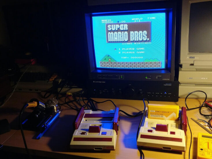
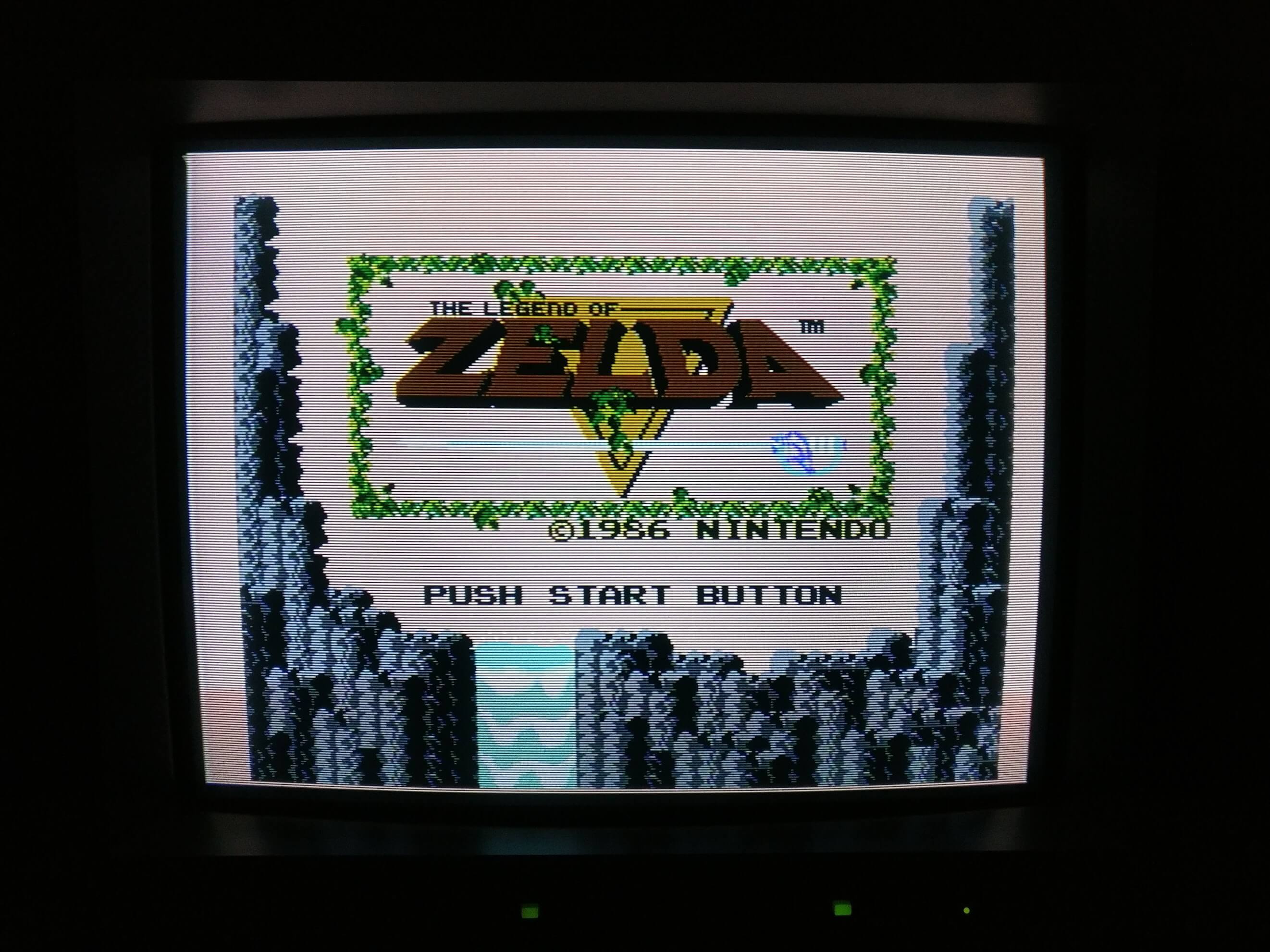
If video isn’t your thing, here are a couple of pictures taken from my 17” JVC PVM type CRT monitor. It’s a CRT, so please ignore the weird banding and lack of sharpness on some of the pictures, the picture is pretty much perfect in real life.
Please click on the images to see the original unedited photos.


…If that’s the kind of picture you’re looking for at the cost of a few basic components and an hour or so with the soldering iron, read on. If not, I wish you all the best in your quest! There are links to plenty of reading material at the bottom of this page if you want to do some further research.
If you’re looking for a true RGB output perhaps Tim Worthington’s NESRGB is more your kind of thing? It’s available from oldskoolconsoles in the UK for £90 (at time of writing). No affiliation at all and I haven’t installed one myself (yet) but I like to be transparent about the various options.
Note that the output of this mod will use the Famicom’s native NTSC signal. This is the TV standard used in Japan* and the US. Outside of these countries most modern TVs should be able to accept this signal over a composite connection but it might be worth checking compatibility with your TV first.
* I’m well aware that the Japanese variant of NTSC is called NTSC-M. For our purposes the differences are immaterial.
Shopping List
Here are the components I used for this mod:
- A1015 Transistor (or equivalent PNP transistor)
- C1740 Transistor (or equivalent NPN transistor)
- 2x 220μF Electrolytic Capacitor (1x video and 1x audio filter caps)
- 1N4001 Diode (the actual part number of the diode is not too important)
- 2200 Ohm Resistor (red red red gold)
- 220 Ohm Resistor (red red brown gold)
- 82 Ohm Resistor (grey red black gold)
- 68 Ohm Resistor (blue grey black gold)
- Thin gauge insulated wire
- 2x 1μF capacitors for PPU / CPU noise suppression (optional but recommended)
- Heat shrink (optional)
I also bought a cheap 1.5m component cable, but others drill holes in the case to mount the connectors or install a 3.5mm socket. If you’re capable enough to perform this mod then I will leave that decision in your hands. I have included some examples for inspiration further down the page.
It may be possible to substitute some or all of these components, particularly the transistors, but above are the part numbers that I use. The resistor values above generally give the best results but feel free to experiment.
Easier Alternative - IMPORTANT
It’s now early 2025, and the world has changed a great deal since I wrote this guide 6 years ago. For example, there is now an SMD video amplifier circuit available that is tidier and easier to install:
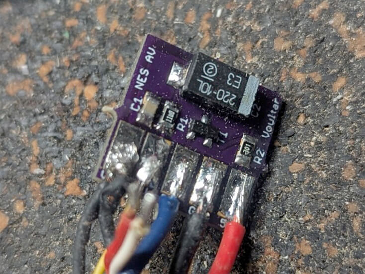
I can’t offer any advice on this particular mod as I have no experience of it myself, but I can certainly vouch for Voultar’s credentials in this field. Of course, the steps detailed below about dismantling the Famicom, lifting the PPU pin and interfacing to the outside world still apply when using one of these AV boards.
I won’t link to specific suppliers as things change fast (unlike this page) but some search keywords might include “nes av”, “famicom av”, “voultar”, “mod”, and “composite”. The board pictured above was purchased on eBay UK for £13.99.
Thanks to Fuzzweed over on BlueSky for the tip and above image.
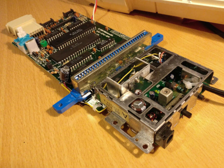
Famicom Disassembly And Motherboard Identification
Before we start we need to open up the Famicom. First remove the 6 screws on the bottom, and then extract the motherboard by removing the 8 screws that hold it to the top part of the case. Remove the 2 screws holding the power switch in place, and finally, you’ll also want to unplug the controllers. Now the motherboard should just lift out.
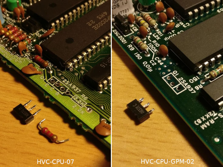
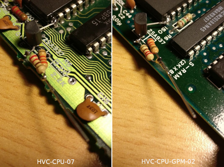
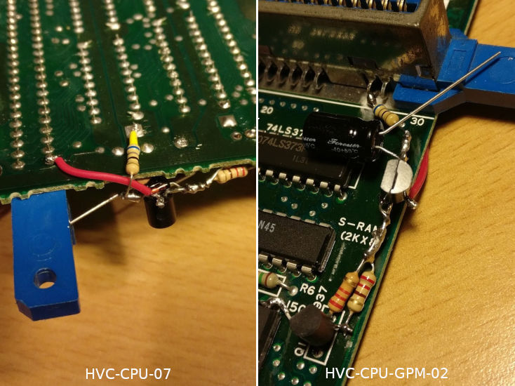
There are 2 different motherboard revisions:
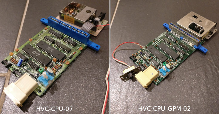
On the left we have the original HVC-CPU-07, dating from 1983, and on the right the later HVC-CPU-GPM-02 which seems to have been used from 1989 onwards. It seems that the video and power circuitry is better shielded on the later revision and the power supply has been simplified. My uneducated guess is that this was done to comply with changing RF emissions regulations, and also maybe to try to reduce interference internally and improve the video and audio output. It doesn’t really matter which motherboard you have for the purposes of this mod, the end result is the same.
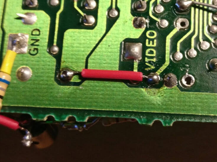
The HVC-CPU-GPM-02 actually has a pad marked “video” on the bottom which some have tapped into and reportedly had good results, but for the purposes of this guide I’ll be bypassing this and performing exactly the same mod on both motherboard versions.
Explanation Of The Mod
Feel free to skip this part if you already know what we’re trying to achieve here or if you just want to get into the instructions and get on with it.
The two large chips on the board are the PPU (Picture Processing Unit) and CPU. If you’re familiar with PCs and modern consoles, the PPU is basically equivalent to the GPU. This chip deals with drawing graphics to the screen and then natively outputs this to a composite video signal, which is usually routed via traces on the motherboard to the power / RF board and converted into an RF signal to be fed to a TV.
The problem is that the Famicom’s circuitry isn’t all that brilliant. The power supply is noisy, the PCB trace that takes this video output from the PPU is routed right next to one of these noisy power lines, and the chips themselves are old NMOS chips which emit more than their fair share of RF to begin with. This can all manifest itself as a type of interference called “jailbars” which are faint vertical lines that appear across the screen. For years they were an accepted part of Famicom modding, but they absolutely can be avoided if you’re careful.
It’s been known for a while that the way to get the cleanest possible signal is to start with the native NTSC composite output from pin 21 of the PPU and take it from there. So here is the schematic for the bulk of the circuit that we will be adding, which is the video output from the Sharp Twin Famicom console as drawn up by user deadbody on the NESDev forums. PPU pin 21 is on the left. Take a moment to take it all in:
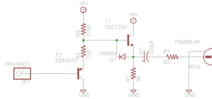
In my implementation of this mod we route the video signal straight away to the outside of the motherboard immediately to try to avoid picking up any interference, particularly those horrible jailbars I mentioned earlier. Then the circuit cleans it up a bit more for good measure, gives it a bit of a boost, and passes it through to the outside world via a standard yellow RCA connector.
While we’re at it we can also pick up the audio signal and send that out along the same cable for the complete package. Thankfully audio is much more forgiving and minor interference is somewhat less obvious, although we can filter that a bit as well just for good measure.
Step-By-Step Guide
Please read the instructions and look at the pictures from start to finish before beginning. I won’t be held responsible if you mess this up!
It should be noted that space is tight above, below, and to the side of the motherboard. I find that keeping the top and bottom parts of the case nearby and constantly checking the position of components is much easier than having to move things once everything is soldered in place.
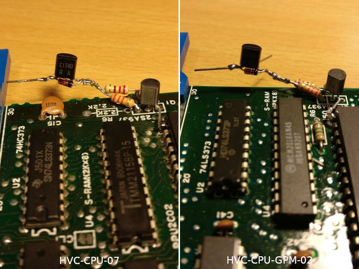
Step 1 - Removing The Old Video Output Transistor And Cutting / Lifting Pin 21 Of The PPU
First we need to remove the small square transistor (labeled 2SA937) close to the PPU, and then decide how we’re going to deal with pin 21 of the chip itself. This is the pin on the corner closest to the transistor. Some guides say to leave it soldered in place and cut the trace running to it, while I have recommended cutting this pin in the past (as pictured above).
Following some feedback from Fuzzweed over on BlueSky I would now recommend carefully desoldering and lifting this pin if possible, with one caveat: it is possible to shear off the pin completely if you overwork it, so if you’re not feeling confident, perhaps cutting it would still be the best cause of action.
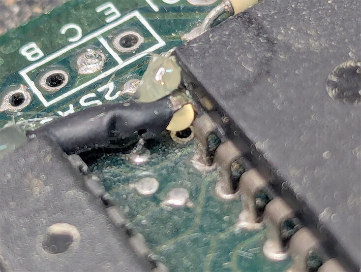
As you can see in Fuzzweed’s photo above, he has also used some hot glue and heat shrink tubing to reinforce the pin and protect from short circuits. Very tidy solution!
If you do go down the route of cutting the pin, leave enough poking out of the chip that you can solder to - this method is irreversible so don’t mess it up! I then desolder the remains of the pin from the motherboard, leaving a hole. This will prevent solder from re-joining the connection later.
On the HVC-CPU-07 motherboard I have also removed the resistor labeled R6. This is a 2200Ω so you could reuse it if you want to save a few pennies.
Step 2 - Adding The New Video Output Transistor
Some mods reuse the original transistor that we just removed but I prefer to replace it. Looking back at our circuit diagram above, we can see that the Sharp Twin Famicom uses a 2SA1015 transistor, so that’s what I’m using here. I’m assuming here that you used my shopping list above and have one of these (or equivalent) PNP transistors handy.
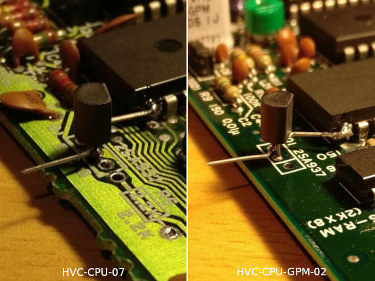
The next step is to solder this in - make sure you picked up the right one as the two transistors aren’t interchangeable! This is a PNP transistor, so with the flat side facing inwards towards the PPU, bend the pin closest to the PPU so that it touches pin 21. Bend the leg at the opposite end outwards so that it is pointing in the opposite direction, off the edge of the board.
Poke the centre leg through the centre hole of the transistor that was just removed (labelled “C” for “Collector” on some motherboards) and solder it in place. Finally, solder the leg closest to pin 21 to the pin.
Please follow the pictures above for reference as this step is quite fiddly.
Step 3 - Adding The Resistors
Now we add our resistors. I like to pick up 5V from one of the pins of the original transistor that we replaced in step 1. This is labelled “B” (for “Base”) on some motherboards. If you’d rather not do that there are some other places nearby, so feel free to have a poke around with a multimeter and see what you can find. One leg of the 2200Ω resistor goes here. If you are using the Base pin as I do, be sure that there is no way for the leg of the resistor touch the new transistor above it.
One leg of the 220Ω resistor attaches to the third and final pin of the new output transistor that we added in the previous step.
Finally, tie the other legs of the resistors together. I know the pictures here aren’t overly clear but it should be pretty self-explanatory.
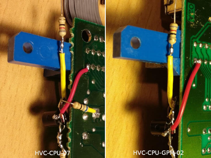
Step 3a - Note On HVC-CPU-07 Motherboard
Note that this step only applies to the HVC-CPU-07 motherboard (separate RF / power board with ribbon cable). In the original version of this post I mixed these two up. This section has now been updated - sorry for the confusion!
I like to reuse one of the original transistor holes for the 2200Ω resistor as it makes for a tidier job and a much more mechanically secure mounting. It also keeps things compact as space is very tight around this area. The trouble is that on the HVC-CPU-07 this will no longer be receiving power after removing the R6 resistor in step 1.
The solution, as pictured above, is to add a short bridging wire (red, centre of picture). You may notice that there are some additional components in this picture and that this wire is missing on some of the following pictures - this is because I added it out of order when taking photos, but I recommend adding it now so that it doesn’t get forgotten.
Step 4 - Adding The NPN Transistor And Diode
Now we start on the amplifier and filter part of the circuit. We need to add a diode across the two outer legs of the second transistor (the 2SC1740). The component I found was small enough to fit neatly across the bottom, but some diodes can be much bigger. Start by bending the two outer legs of the transistor outwards in opposite directions, and the centre leg out at a 90 degree angle, away from the flat side.
This is going to be hard to explain, so study the pictures to see which way around the diode goes - notice that one end is marked, and this end is connected to the same side of the transistor as the resistors that we just added.
Now with the flat side of the transistor facing inward (again, so it is in the same orientation as the one we previously added), solder the leg closest to the resistors to the resistors themselves.
Step 5 - Powering The NPN Transistor
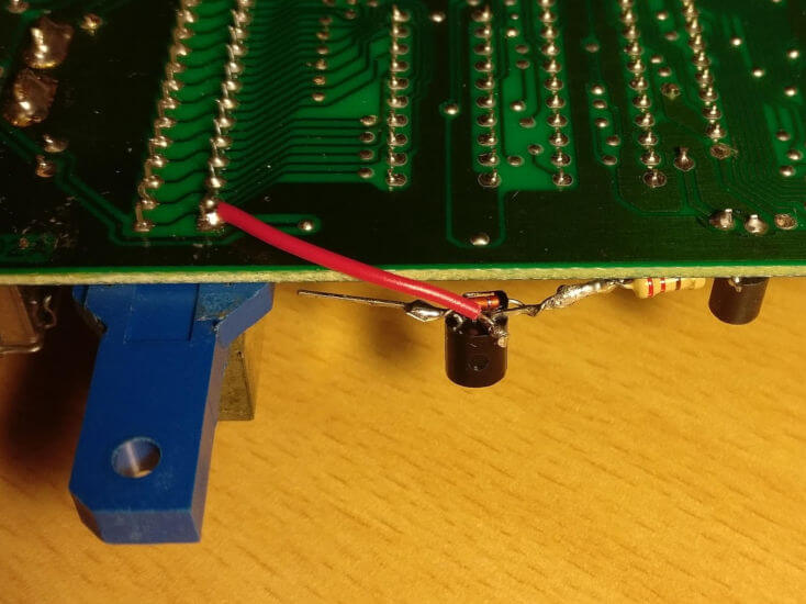
The collector (middle leg) of this transistor needs a 5V source. There are a couple of places on the motherboard nearby where this can be picked up but I find that the easiest place is pin 30 of the cartridge slot, which handily is the corner closest to these components.
Flip the board over and attach a short length of insulated wire as pictured. This is exactly the same for both motherboard revisions.
Step 6 - Grounding The NPN Transistor And Adding The Video Filter Capacitor
Now we need to ground the third and final leg of the newly-added transistor using a 68Ω resistor. If things are going to plan this should be the leg pointing towards the cartridge slot end of the board. On the HVC-CPU-07 solder the resistor to the GND pad on the bottom as pictured above - I used a tiny section of heat shrink here to prevent shorts but it’s probably not entirely necessary. If you’re concerned you could also add a small piece of electrical tape.
The HVC-CPU-GPM-02 motherboard lacks the ground pad on the underside but a nearby ground is easy enough to pick up from the cartridge slot shield on the top side.
We also solder the positive leg of a 220μF electrolytic capacitor to this same transistor leg. Electrolytic capacitors have a line on one side which marks the negative side of the component - so be sure to use the opposite leg.
Note that space is tight around the cartridge port and the capacitor is a larger component so check for fit using the top part of the case. I prefer to position the capacitor as pictured but it will be against the cartridge port moulding here so be careful.
Step 7 - Adding The Video Output Resistor
Finally we need to add our remaining 82Ω resistor to the negative leg of the 220μF capacitor that we just added in step 6. This brings our final composite video output to the correct levels and will be where you will connect the centre pin of the yellow RCA connector.
I like to cover the leg of the capacitor with some heat shrink, as it can inadvertently be pressed against the other components when replacing the top part of the case which could cause a short. I also feed it around the bottom of the blue structure of the cartridge slot as pictured. Please ensure that it is tight against the side of the motherboard so that it doesn’t foul the eject mechanism - it can be tied to the hole in the corner of the motherboard to keep it out of the way if necessary as this hole isn’t used and has plenty of clearance.
Now the video part is done! I like to give it a quick test at this point just to make sure that everything is functioning as expected before continuing.
When connecting the RCA connector the outer sleeve needs to be grounded - see the note below under “Audio Output” to see where I usually connect this, but any of the ground connections we’ve used so far or even the outside of the RF shield would work just fine.
Step 8 - CPU And PPU Decoupling Capacitors
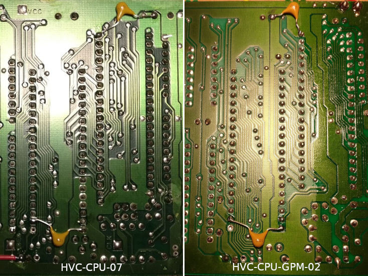
Hint: The blue cartridge slot is to the left hand side in the above pictures
Previous modders around the internet have found that adding capacitors to the places pictured above will help to clean up the video signal and reduce those pesky jailbars. I have to say that after some experimentation I’m in agreement and think that they are worth the effort - as long as they’re in the right places. These act as decoupling capacitors and clean up any electrical noise from the supply feeding the CPU and PPU.
Recommendations on the values vary, but I find that a couple of 1μF ceramic capacitors are sufficient. As they’re ceramic it doesn’t matter which way around they go. They should have the code “105” on the outside.
Please double and triple check that you have connected these to the correct pins as pictured, and that the legs aren’t touching any other solder pads or components.
Audio Output
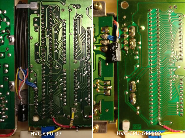
There are a couple of places to pick up the audio output, but after some experimentation I finally decided to use the connectors where the power / RF board connects to the mainboard. The good thing about these pads is that they are labeled. Add a 220μF capacitor here, with the positive leg connecting to the pad labeled “A”. The negative leg of the capacitor then connects to the centre pin of the audio RCA connectors.
Some people use pin 46 of the cartridge port, which works just fine as well and may make more sense if you are adding your RCA connectors to the side of the console as it will be closer to where you want to be. There’s an argument that as the “source” of this signal picking up from this pin should be less prone to interference, but to be honest we’re well away from those NMOS chips here and I personally haven’t found it to be any better.
Finally, the outer sleeve of both the video and audio RCA connectors need to be connected to ground. I use the same grounding point for all 3, which is another one of the pins on the same connector (the blue wires pictured above).
Interfacing To The Outside World
My Solution
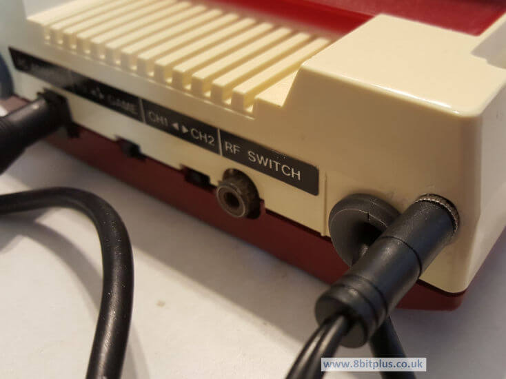
I clamped my motherboard in a workbench and used a hacksaw to cut a square hole around where the original RF connector was, and then desoldered it. It could also be drilled out, I suppose. Either way it can be removed as it’s not functional after this mod anyway (as with all of the switches on the back).
Then the new cables can be carefully routed through this box, cable tied to protect the connections, and run out of the “RF Switch” hole on the back of the console for a nice tidy job.
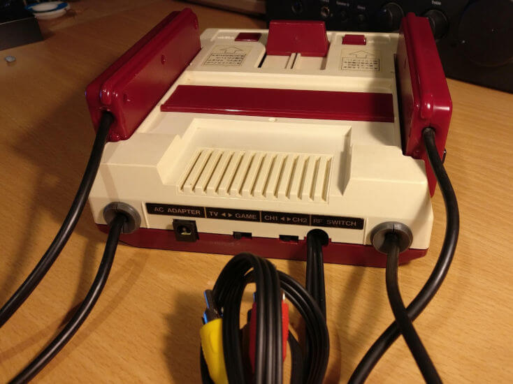
The Famicom has a load of cables all over the place anyway, what’s an extra one…
Other Interface Solutions
I took the above photo from this boards.ie post. Personally I’m not keen on this solution as I think my version preserves the original looks of the console (at least from the front), but it is very neat and does allow different composite cables to be used depending on distance from the TV. It’s certainly worth considering.
This one shows 8bitplus’s solution. I really like the idea of mounting a 3.5mm jack discretely on the back of the case and may well have to borrow this idea in future. It could even be mounted in place of the original RF connector to make it even more seamless.
Troubleshooting / Potential Improvements
If you’re still seeing “jailbars” (thin white vertical lines) on the video output then your Famicom may have a particularly noisy PPU or power supply. Step 5 of the original jpx72 post covers using copper tape to reduce emissions from the PPU by essentially creating a Faraday cage around the chip. It involves desoldering the chip so it’s quite involved. Personally I’ve never tried this as I’ve been very happy with the consoles I’ve modded so far, but I thought I’d include it here for reference.
You could also try tweaking the values of some of the capacitors and resistors. I’ve found that increasing the value of the decoupling caps on the back of the CPU and PPU in particular can help - up to a point. Electrolytics could also be used here, but be sure to get the polarity right (hint: the multimeter is your friend). You could also try different values for the filter caps on the final stage of the audio and video outputs, bigger is not necessarily better in this case.
It probably goes without saying, but if you’re getting no output at all double and triple check your work - in particular make sure the transistors and capacitors are the right way round. Make sure your connections aren’t shorting out and that the solder joints are strong. Probe the 5V connections with a multimeter and make sure you’re getting power to the right places. If you have the HVC-GPM-02, check that you added the small bridge wire in step 3a.
If your controllers or anything else are behaving erratically make sure you definitely added the PPU and CPU decoupling capacitors in the right places. I have accidentally soldered these to the wrong pins before and while the Famicom initially appeared to work, it was glitching out in some unexpected and mysterious ways!
Email Support
I used to offer email support on this mod with a link to my email address here. To be honest, the number of people I could actually help out with troubleshooting in the many years since I published this has been very, very tiny and a few were incredibly rude when this didn’t work.
In honesty I haven’t touched a Famicom since writing this article, and all I’ve really done here is compiled what others have done before me. It was for my own use as much as anything else. I am not an expert.
All that said, I have had a lot of positive feedback on social media from people who’ve carried it out successfully, which is always nice to see.
I’m very limited in the help that I can offer with this, so to manage expectations I have removed my email address. Sorry to disappoint. Your best bet is probably to ask on one of the forums listed below, where this mod actually originated.
Further Reading / References
I’m merely standing on the shoulders of giants with this mod, so here are some sites that I consulted when developing it:
- jpx72’s post is considered one of the most authoritative step-by-step write-ups of Famicom composite mods. I could have just pointed you there, but my version incorporates the Twin Famicom circuit mentioned below as well as a few other tweaks and improvements.
- deadbody’s NESDev Post and the ensuing discussion documented and explained the Sharp Twin Famicom circuit which I have combined with jpx72’s method above to create this mod. There’s some good inspiration for some nice tidy installation options here.
- Myrddin’s boards.ie post covers some others’ attempts at composite mods and was a useful reference when developing the finer points of this mod.
- Japanese model rail enthusiast stevenh’s blog documented his version of this mod and is where I got the inspiration for the decoupling capacitors on the CPU and PPU. He has some very clear step-by-step pictures and reuses the original PPU pin 21 transistor for his mod.
- 8bitplus documented their version of the mod. They’ve used different values for the components and the positioning is a bit too close to the noisy PPU and CPU for my liking. It seems to be based on a very early version of the Famicom composite mod from a website called jpxdetail which I have found referenced elsewhere but is no longer online. The poster reports that jailbars are still prominent with this mod and their pictures seem to show that this is indeed the case.
- dxprog’s FamicomPowerBoard project on GitHub is a very comprehensive upgrade that completely replaces the Famicom’s original power and RF board. I didn’t use any elements of it in my mod but did come across it on my travels and was very impressed. I’m definitely hoping to try this one in future.
If you liked this post please consider following me on Instagram or BlueSky!